The term electrical conductor is used for all materials which have charge carriers (such as valence electrons in metals), which can conduct the electrical current. Electrical conductivity? (sigma) – aka conductance value – is a material-specific parameter. It describes how well a material can conduct an electrical current. The inverse of specific conductivity is specific resistivity? (rho). It expresses the amount of resistance a material exerts against the flow of charge carriers. To determine these material parameters the probe geometry (length and cross-sectional area) and electrical quantities (voltage drop and current strength or resistance) are linked together:
σ – Specific conductivity in S / m
(Siemens / m, 1 m / Ω mm2 = 1 MS / m) ρ – Specific resistivity in Ω mm2 / m
U – Voltage drop in V (volt)
I – Current strength in A (ampere)
R – Ohmic resistance in Ω (ohm)
– Length of the conductor in m
A – Cross-sectional area of the conductor in mm2
In Anglo-American regions electrical conductivity is indicated using the IACS system.
The specific conductivity, and thus also the specific resistivity, are temperature-dependent.
In the case of metals specific conductivity generally drops with rising temperature, because the increasing thermal movement of the atoms generates more resistance to the flow of the charge carriers.
Impedance of coils
In eddy current testing one uses a coil to generate (induce) eddy currents in the product to be tested and record the feedback from the product, which reflects the product’s properties.
In the simplest case, an eddy current probe consists of only one coil, which acts as both sender as well as receiver (parametric probes). The operational principle consists of the product to be tested impressing its properties on the coil – or to be more precise, on the coil impedance.
Impedance is understood as resistance to alternating current. In a coil it is composed of 2 components: The ohmic resistance R (this corresponds to the DC resistance of the coil wire and is constant; i.e. independent of frequency) and the inductive reactance XL, which is produced because the coil wire is wound into turns. Provided a coil is traversed by an alternating current, the coil turns are within the area of influence of their own magnetic field. Consequently, currents are induced in them which flow in opposition to the causative coil current and superimpose themselves on it. The resulting overall current is thus phase-shifted; i.e. time lagged.
Ohmic resistance is dependent on the geometry and material of the conductor wire:
– R – Ohmic resistance in Ω
– l – Length of the conductor in m
– A – Cross-sectional area of the conductor in mm2
ρ – Specific electrical resistivity in Ω mm2 / m
The inductive resistance XL is greater:
– The higher the frequency f, and
– The larger the inductivity L of the coil
and can be calculated with the following formula:
XL – Inductive reactance in Ω
f – Frequency in hertz (Hz = 1 / s)
L – Inductivity in henry (H).
The coil inductivity is dependent on the coil turns, the coil dimensions and the material forming the interior of the coil:
L – Inductivity in H (henry, 1 H = V s / A)
μ – Magnetic permeability in the coil interior in V s / A m (with μ = μ0 * μrel)
n – Coil turns
A – Cross-sectional area in mm2
l – Coil length in mm
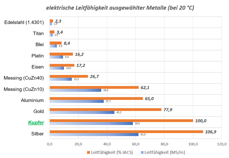
A unit of electrical conductivity that is particularly common in the USA is the IACS (for International Annealed Copper Standard). Here, the electrical conductivity σ is expressed as percentage of the conductivity of electrolytically refined pure annealed copper (with 58 MS/m). For the conversion from SI units to the IACS system the following applies:

An electric conductor traversed by a current is surrounded by a circular magnetic field (eddy field). If the straight conductor wire is now wound into a circular conductor loop, the eddy field lines overlap in such a way that they form a magnetic dipole (with north pole/south pole structure).
The strength of the magnetic field generated can be increased by winding the coils, just as they are used in eddy current testing as probe elements, with a larger number of coil turns. With increasing coil length their magnetic field becomes more and more like that of rod-shaped permanent magnets.
The magnetic field outside of the coil penetrates the electrically conductive product to be tested. Since the coil is traversed by an alternating current, circular currents are induced close to the surface of the product to be tested, which are called eddy currents.
These eddy currents run counter to the direction of the coil current, and can in a sense be understood as mirror image of the coil current. The flowing eddy currents in turn are surrounded by a magnetic eddy field.
In a “defect-free” test specimen (homogenous material) the eddy currents can propagate unimpeded.
The magnetic field generated by the eddy current, too, is characterized by a dipole structure. This secondary magnetic field is in opposition to the primary magnetic field of the coil. The superimposition of both magnetic fields leads to a resulting magnetic field, which, compared to the primary magnetic field of the coil, has a smaller field strength.
Should the product to be tested have any local defects (e.g. cracks, corrosion pits, pores, non-metallic inclusions or similar), the eddy currents won’t be able flow unimpeded anymore. In a sense, such inhomogeneities represent an insurmountable obstacle. The eddy currents must go around to the side and/or in direction of depth, and therefore experience a weakening. Consequently, the magnetic eddy field around them is also weakened. The reduced magnetic counter-effects on the primary field of the coil lead to changes in the resulting magnetic field so that it differs from that of the defect-free test specimen.
The strength of the magnetic field under the influence of an electrically conductive product can be registered by suitable probes (receiving coils), then analysed, and displayed in a suitable way. This way, conclusions about the properties of the test specimen can be drawn, for example regarding geometry, dimensions, material parameters and the presence of local defects.
Because of the “skin effect”, the strongest eddy currents form on the periphery of the product to be tested; with growing distance from the periphery their strength drops rapidly. That is why eddy current testing is categorized as surface technique, which principally can be used for all electrically conductive materials.
Since the nature of the eddy currents is affected by numerous properties of the product to be tested, there are diverse fields of application for eddy current testing (e.g. testing for material defects, determination of wall thickness, measurement of material characteristics for sorting purposes, measurement of layer thicknesses, and many more). Compared to other non-destructive testing methods the eddy current method is characterized by the following benefits:
– Contactless,
– No preparation or subsequent treatment of the surface necessary,
– No coupling media necessary,
– High testing speeds possible (up to several m/s).
With such characteristics, it is highly suitable for use in automated testing systems.
On objects made of electrically conductive materials eddy current testing can be used to test for integrity, composition and tempering quality, or also for geometric dimensions. In the process it exploits the physics of electromagnetic fields. Its application is thus contactless and requires no coupling media.
A coil traversed by an alternating current forms a (primary) magnetic field in its surroundings. As a result of this, currents form on the surface of the electrically conductive product to be tested. Known as “eddy currents”, they flow parallel to the coil turns, but in the opposite direction of the coil current. That is why they generate a (secondary) magnetic field, in the opposite direction of the magnetic field of the coil. This ultimately produces a weakening of the magnetic field of the coil. This can be measured as change to the alternating current resistance of the coil (impedance).
Should the product to be tested have any local defects (e.g. cracks, non-metallic inclusions, pores, corrosion pits), the eddy currents won’t be able flow unimpeded anymore. With that, the value measured on the coil changes in comparison with a product that is defect-free. As the probe slides along the product to be tested the high-frequency carrier signal of the eddy current coil (HF, excitation frequency) is modulated, which means the signal level varies. For the displayed example of a crack, the signal level increases. With the help of demodulation a low-frequency signal (LF) is acquired, which contains the information about the product to be tested, including any possible defects.
Based on the variations in coil impedance it is thus possible to record and characterize the properties of the product to be tested (insofar as they have an influence on the nature of the eddy currents), including any possible defects. Specific analysis methods are required for this, such as amplitude or phase analysis, signal form analysis or harmonic analysis. Before testing begins the eddy current instrument must be configured (excitation frequency, amplification, phase settings, filter settings, etc.) with the help of reference objects, which must possess certain properties in terms of geometry (dimensions, shape), material parameters (electrical conductivity, permeability, hardness), and material defects. To ensure reliable test results the test conditions must be adhered to while testing is in progress (e.g. constant probe distance and uniform testing speed). All perturbations (e.g. mechanical vibrations, temperature fluctuations, or electromagnetic fields) should also be ruled out, or minimized as much as possible.
Another important requirement for successful eddy current testing is the choice or development of a suitable probe; this includes the number and arrangement of the coils used, the type of electrical wiring, their dimensions, number of turns, a magnetic core if necessary, or shielding.
Low-pass filters are used to suppress interfering high-frequency signal components of the frequency spectrum, while frequencies below a lower cut-off frequency (i.e. the signals of interest) remain unaffected (see also bandwidth). This type of filter is also known as static filter, because the frequency spectrum of the demodulated signal also contains a constant (static) component.
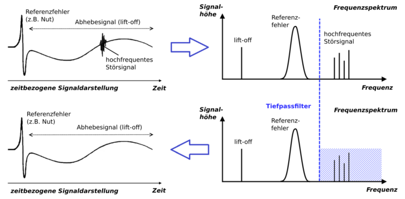
Low-pass filters are used to suppress high-frequency electromagnetic interference, for example, but also electronic device noise. It should be noted that the frequency spectrum of the interference signals and the signals of interest depend on both the actual testing speed as well as on the type and geometry of the probe used: the faster the testing speed and the smaller the length of coverage of the coil used, the higher the frequency of the signals (-> “shorter pulses”). For lower testing speeds and for relatively large coil dimensions the frequencies of the signals are correspondingly lower (-> “longer pulses”).
The lower cut-off frequency of the low-pass filter is correct (i.e. set high enough) when the signals of interest are displayed at maximum signal level. The minimum lower cut-off frequency fTPmin for the low-pass filter can be approximately determined with the following formula:
fTPmin > vtest / Bw
(with: vtest = testing speed, and BW = length of coverage of the coil).
The art of probe development consists of realizing a probe construction that can apply the required magnetic field (and with that the eddy current field) at the necessary excitation frequency with optimum alignment and the required strength to the location to be tested in the workpiece, but always minimizes unwanted effects as much as possible. Basically the best test instrument can only gather the information that the sensor technology can acquire in the first place. A “blind” probe cannot facilitate sensitive testing. Another decisive factor in addition to this basic sensitivity is the exact reproducibility of the probes.
Probe multiplexing means that multiple probes (or multiple test coils) are operated quasi-simultaneously with the same set of test parameters (excitation frequency; amplification, phase and filter settings; gates, etc.). Technically speaking, a multiplexer (MUX) is used to quickly sequence through the individual probes. This means that each individual probe is only operated for a short duration.
Multiple probes or array probes can be operated very efficiently this way. To scan a test surface two dimensionally, for example, all that is necessary is to scan it mechanically in one direction. The second dimension is covered by “virtual scanning” via multiplexer (electronic shifting in a fixed time frame).
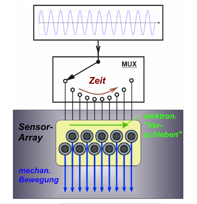
Probe multiplexing allows considerable time savings compared to the single-probe method. It also allows a considerable reduction in hardware outlay in comparison to conventional testing technology (lower number of testing modules and instruments necessary). As opposed to simultaneous multi-probe testing there is a reduction of mutual interference (crosstalk). The use of array probes thus allows the testing of relatively large surfaces with high measurement sensitivity and local resolution in the shortest of times.
Segmental probes represent an intermediate stage between the two basic types, coaxial probes and surface probes. They don’t completely surround the product to be tested, but they do usually cover a wide circumferential area between 90° and 180°. Their resolution capacity lies somewhere between that of a coaxial probe and a surface probe.
In the choice of excitation frequency the requirements of the application and the probe to be used must be taken into account. The frequency range recommended for the probe can be found in the manufacturer’s data sheet for the probe.
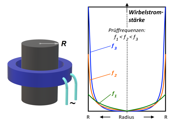
The excitation frequency has a decisive effect on depth detection capability; i.e. the distribution of the eddy current strength in the direction of depth:
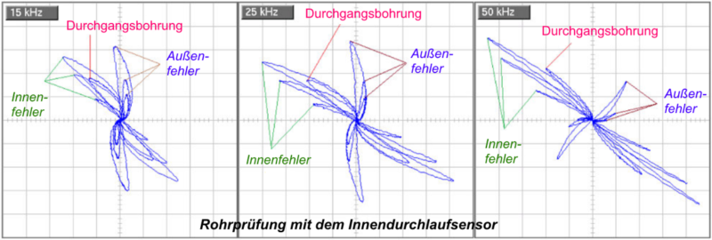
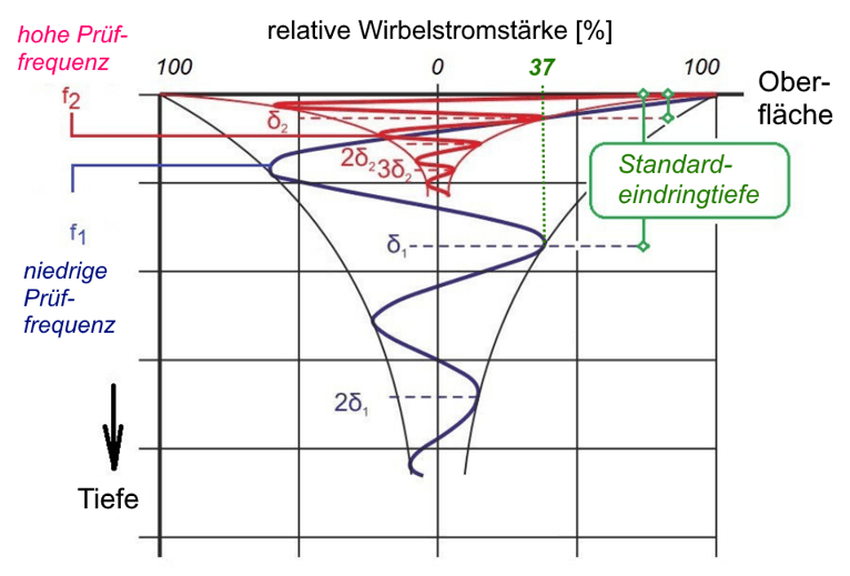
With increasing distance away from the surface the eddy current strength drops considerably. The eddy currents concentrate themselves largely on the surface; they are shielded to some extent in the direction of depth. This is known as the “skin effect”. One measure of the drop in eddy current strength with depth is the standard penetration depth. The higher the excitation frequency, the larger the strength of the eddy currents induced on the surface of the product to be tested (according to the law of induction). But on the other hand, the higher the excitation frequency, the more the eddy current strength drops in the direction of depth. (Note: The electrical conductivity and the relative permeability of the product to be tested have the same influence on the distribution of eddy current strength as does the excitation frequency.) For that reason, with the choice of frequency it is possible to exercise specific control on the measurement sensitivity as well as the zone of interaction (volume penetrated by eddy currents): High excitation frequencies generate strong eddy currents at the surface of the product to be tested and so they offer excellent sensitivity for surface defects. Because of their better penetration capacity, low excitation frequencies offer good sensitivity (detection capability) for defects lying under the surface (concealed defects). The choice of excitation frequency also has an influence on the phase separation angle of defects of different depths. This can be exploited for example in the examination of pipes using an internal coaxial probe (aka “bobbin”) with phase analysis: At low excitation frequencies the directions of signal drift (phase angles of signals) of internal defects of different depths or external defects of different depths hardly differ from one another. At increasing excitation frequency the separation angle of defects of different depths grows. This corresponds to better resolution capacity in the direction of depth. (Note: The electrical conductivity and the relative permeability of the product to be tested have the same influence on the phase separation angle as does the excitation frequency.)
Parameter-multiplexing means that a probe is operated sequentially with multiple test parameters. To this end the individual parameters are switched between in rapid succession and each is only active for a very short duration. This way it is possible to perform a multifrequency examination, for example. Naturally it is also possible to switch to other test parameters, according to a defined time frame (filters, gates or similar). Major advantages include considerable time savings and the reduction of hardware requirements compared to conventional methods. In comparison to simultaneous examinations, even the effects of mutual interference (crosstalk) between the measurement channels are reduced.
Compared to single frequency examination, multifrequency examination offers more possibilities for signal analysis. This means that it offers a considerable information “bonus”, so it leads to an increase in the reliability of examination conclusions.
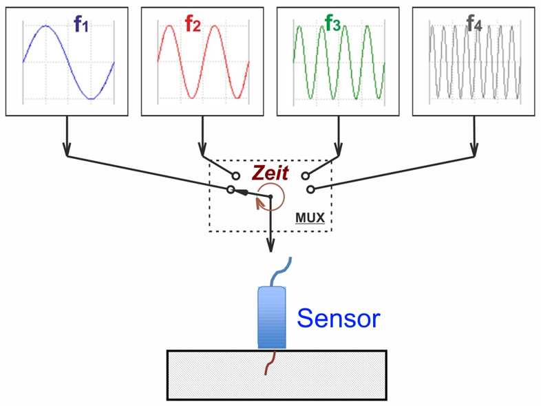
Multiplexing (aka MUXING) is a method of serial transmission of multiple signals over a shared medium. In the process all signals are apparently transmitted simultaneously. Strictly speaking, however, they are transmitted “one-by-one” as it were, in alternation in time slices. The shared transmission channel is divided into time slices. A time slice is allocated to each signal. To transmit, a multiplexer (MUX) sends one signal after the other to the transmission link, each for the duration of one time slice. At the other end of the link a demultiplexer (DEMUX) synchronously sends the transmitted signals to the associated recipients. A complete multiplex cycle consists of the sum of all time slices. A defining variable in multiplexing is the multiplexing rate. It corresponds to the inverse of the cycle time and is an expression of the number of signal channels that can be transmitted per time unit (usually per second). The particular advantages the multiplexing method offers include the reduction of hardware costs (fewer measurement channels and less cable), the reduction of space requirements (multiple probes can be run with one instrument, thinner cable), considerable time savings (with multifrequency examination or the use of array probes), and the prevention of interference or crosstalk between the channels.
On the other hand there are disadvantages: Under certain conditions seamless scanning cannot be guaranteed anymore at high testing speeds (at multiplexing rates that are too low); also poorer signal quality (signal-noise ratio), because at increasing multiplexing rates less and less data points per time slice are available.
In eddy current testing one differentiates between the following types of multiplexing: Parameter-multiplexing (e.g. as multifrequency examination) and probe multiplexing (switching over to multiple probes or running array probes).

High-pass filters are used to suppress interfering low-frequency signal components of the frequency spectrum, while frequencies above an upper cut-off frequency (i.e. the signals of interest) remain unaffected (see also bandwidth). Examples of uses for high-pass filters in eddy current testing include the suppression of conductivity or permeability variations, geometry variations, but particularly also distance signals (lift-off). It should be noted that the frequency spectrum of the interference signals and the signals of interest depend on both the actual testing speed as well as on the type and geometry of the probe used: the faster the testing speed and the smaller the length of coverage of the coil used, the higher the frequency of the signals (-> “shorter pulses”), and for slower testing speeds and for relatively large coil dimensions the frequencies of the signals are correspondingly lower (-> “longer pulses”).
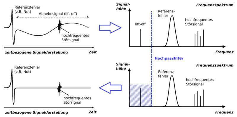
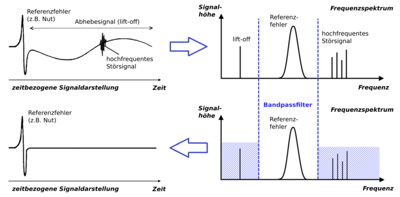
In practice, when performing eddy current tests a series of interfering or unwanted signals can manifest themselves. Examples include variations in conductivity, thermal drift, mechanical vibrations, changes in geometry or lift-off signals. Usually these signals can appear over a longer period of time as defined reference defect (low-frequency signals), as electromagnetic interference, or as electronic noise from the test instrument, which usually appears for a shorter time than a defined reference defect (high-frequency signals). In a worst case scenario the different interference signals can occur simultaneously, so they overlap in such a way that it is impossible to detect and assess the signals of interest (e.g. crack indications) at all anymore. By filtering, it is possible to weaken or eliminate certain frequency components in the demodulated signal. To be able to suppress specific interference signals, the following conditions must be met: firstly the frequency spectrum of the signals of interest and that of the interference signals to be suppressed must be known, and secondly they must differ from one another sufficiently. Moreover, the testing speed must be constant (time-based filter). This way, pseudo-indications or misinterpretations can be avoided and consequently the reliability of test conclusions increased. Available for filtering are the filter types high-pass, low-pass and band pass.

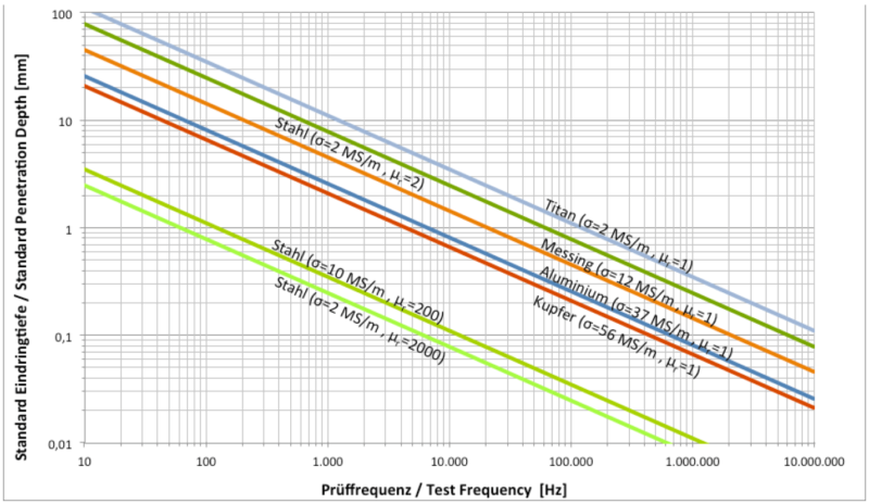
The standard depth of penetration describes the depth (dependent on the electrical conductivity and magnetic permeability of the workpiece, as well as the excitation frequency used) at which the density of the eddy current has dropped to ca. 37%. Penetration performance depends on the nature of the eddy currents. Principally the eddy current field penetrates very deeply into the workpiece at low excitation frequencies, and at high frequencies it only forms near the periphery. Technically, tests at up to 3 to 5 times the standard penetration depth are possible. The following figure depicts standard penetration depths of various materials, based on the excitation frequency. Put simply, with the excitation frequency one can adjust the depth resolution of the eddy current test.
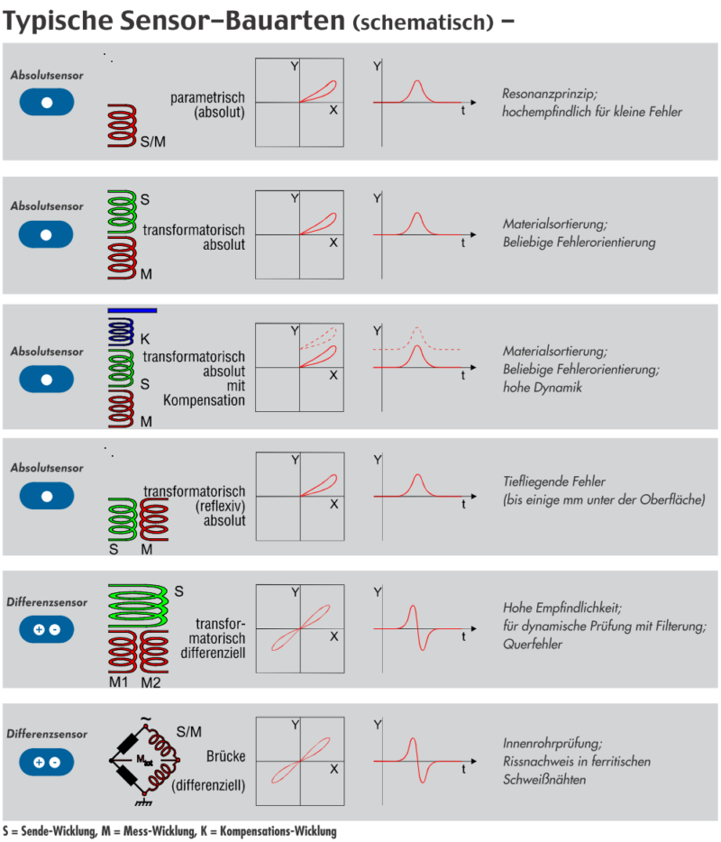
Basically, one distinguishes between two main groups of probes: coaxial probes and surface probes. In the case of coaxial probes one distinguishes between encircling coils, which surround the product to be tested and through which the product is fed (e.g. inspections of rods with surrounding test coils), and internal coaxial coils, which are enclosed by the product to be tested; i.e. the coil is fed through the product to be tested (e.g. inspections of pipe interiors). Coaxial probes always cover a full circumferential section of the product to be tested, either external or internal.
In differential probe systems the same coil arrangement is used as in the comparative measurement method with external reference, only the coils are arranged in such a way that a specific point of the product being tested is compared with another point that is only a short distance away on the same product.
In this arrangement the product being tested is compared with itself. Since one can assume that there is no significant change or no change at all in the alloy and structure within the short distance that the two receiving coils are apart from one another, only defects which suddenly occur or other inhomogeneities are indicated this way.
As such, material defects of a primarily local nature (e.g. cracks) are found using this method, whereas changes in workpiece properties which occur continuously over the entire length are largely compensated for.
The disadvantage of this arrangement is seen in the probe’s dependence on direction. Whereas lengthwise defects such as cracks that run crosswise to the two receiving coils are reliably identified (since only one of the two receiving coils is always affected), as soon as such defects run lengthwise they are either not detected anymore or only to a very limited extent (the lengthwise defects are now covered by both receiving coils simultaneously). This situation can be helped by an arrangement of multiple receiving coils (aka multi-differential arrangements). But these still have their own preferred directions; i.e. defects with certain orientations are still detected only to a limited extent.
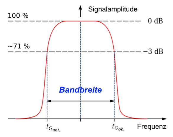
A band pass filter is produced from the combination of a low-pass and a high-pass filter. This means that only a central frequency segment, which only contains the signals of interest, is allowed through unaffected. Only low-frequency and high-frequency interference signals are suppressed. In band pass filters a lower and an upper cut-off frequency are set (see bandwidth). Band pass filters can be used in eddy current testing for example to weaken or eliminate conductivity variations, geometry variations, distance signals (lift-off), as well as high-frequency electromagnetic interference and electronic device noise. It should be noted that the frequency spectrum of the interference signals and the signals of interest depend on both the actual testing speed as well as on the type and geometry of the probe used: the faster the testing speed and the smaller the length of coverage of the coil used, the higher the frequency of the signals (> “shorter pulses”), and for slower testing speeds and for relatively large coil dimensions the frequencies of the signals are correspondingly lower (> “longer pulses”). The use of a band pass filter is also called “dynamic” testing, because the frequency spectrum of the demodulated signal only contains variable (dynamic) content (e.g. rotor applications). This means that the signal point always returns to the coordinate origin, even if the probe is not moved.
Bandwidth is a basic element in signal processing. It describes the range of frequencies in the spectrum; i.e. the frequencies a signal contains. Bandwidth is defined by upper and lower cut-off frequencies. Internally, the upper cut-off frequency is limited in a device by the attenuation characteristics of the system. The lower bandwidth can even be zero. In this case the bandwidth corresponds to the upper cut-off frequency. Typically, one uses the 3-dB criterion, which corresponds to a drop in signal amplitude to roughly 71%. The maximum bandwidth of an eddy current test instrument is an important feature of such eddy current instruments, and is not to be mistaken for the test frequency range that is available. It refers to the frequency spectrum of the demodulated eddy current signal and can be specifically limited to the application-specific requirements using filter settings (high-pass > lower cut-off frequency or low-pass > upper cut-off frequency). This way it is possible to weaken or eliminate interference signals, as long as their frequency spectrum clearly differs from that of the signals of interest (e.g. crack indications).
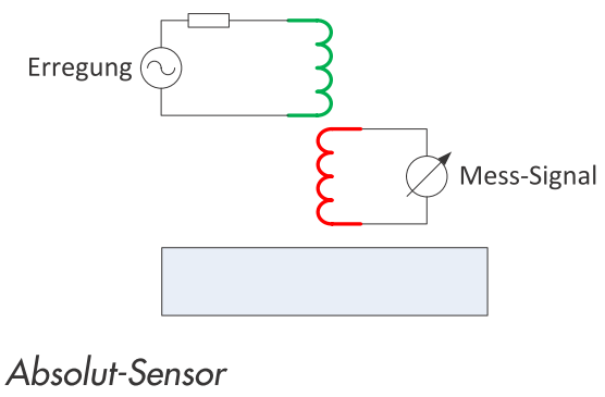
The term “absolute probe” is derived from the fact that the absolute value of the voltage induced in the test coil is measured. The signal of a defect or of a change in the characteristics in the body of the product to be tested is superimposed on the signal of a defect-free product or an empty coil. As such, the test signal is not just influenced by defects, but also by the characteristics of the material of the product to be tested and conditions in the environment. For example, should the probe become warm during operation, its electrical resistance changes and the absolute value of the induced voltage begins to drift. This is the big disadvantage of these probe systems. To suppress disruptive influences such as these or similar, often an additional compensation coil is interposed. It must be arranged in such a way that there can be no interactions with the product to be tested, but so that influences from the environment are effectively suppressed.
